- 您现在的位置:买卖IC网 > Sheet目录2004 > LTC1543IG#TRPBF (Linear Technology)IC TXRX SOFTWARE SELECTBL 28SSOP
5
LTC1543
sn1534 1543fas
C1– (Pin 1): Capacitor C1 Negative Terminal. Connect a
1
F capacitor between C1+ and C1–.
C1+ (Pin 2): Capacitor C1 Positive Terminal. Connect a
1
F capacitor between C1+ and C1–.
VDD (Pin 3): Generated Positive Supply Voltage for
V.28. Connect a 1
F capacitor to ground.
VCC (Pin 4): Positive Supply Voltage Input. 4.75V ≤ VCC
≤ 5.25V. Bypass with a 1F capacitor to ground.
D1 (Pin 5): TTL Level Driver 1 Input.
D2 (Pin 6): TTL Level Driver 2 Input.
D3 (Pin 7): TTL Level Driver 3 Input.
R1 (Pin 8): CMOS Level Receiver 1 Output.
R2 (Pin 9): CMOS Level Receiver 2 Output.
R3 (Pin 10): CMOS Level Receiver 3 Output.
M0 (Pin 11): TTL Level Mode Select Input 0 with Pull-Up
to VCC.
M1 (Pin 12): TTL Level Mode Select Input 1 with Pull-Up
to VCC.
M2 (Pin 13): TTL Level Mode Select Input 2 with Pull-Up
to VCC.
DCE/DTE (Pin 14): TTL Level Mode Select Input with Pull-
Up to VCC.
UU
U
PI FU CTIO S
R3 B (Pin 15): Receiver 3 Noninverting Input with Pull-Up
to VCC.
R3 A (Pin 16): Receiver 3 Inverting Input.
R2 B (Pin 17): Receiver 2 Noninverting Input.
R2 A (Pin 18): Receiver 2 Inverting Input.
D3/R1 B (Pin 19): Receiver 1 Noninverting Input and
Driver 3 Noninverting Output.
D3/R1 A (Pin 20): Receiver 1 Inverting Input and Driver 3
Inverting Output.
D2 B (Pin 21): Driver 2 Noninverting Output.
D2 A (Pin 22): Driver 2 Inverting Output.
D1 B (Pin 23): Driver 1 Noninverting Output.
D1 A (Pin 24): Driver 1 Inverting Output.
GND (Pin 25): Ground.
VEE (Pin 26): Negative Supply Voltage. Connect a 3.3F
capacitor to GND.
C2 – (Pin 27): Capacitor C2 Negative Terminal. Connect a
1
F capacitor between C2+ and C2–.
C2 + (Pin 28): Capacitor C2 Positive Terminal. Connect a
1
F capacitor between C2+ and C2–.
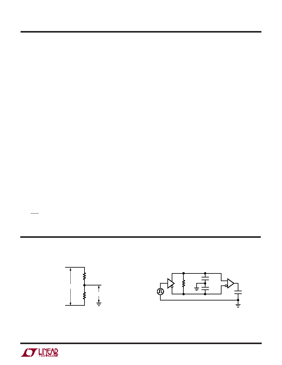
Figure 1. V.11 Driver Test Circuit
Figure 2. V.11 Driver/Receiver AC Test Circuit
A
B
1543 F01
VOD
VOC
RL
50
RL
50
A
B
A
R
B
1543 F02
RL
100
CL
100pF
CL
100pF
15pF
TEST CIRCUITS
发布紧急采购,3分钟左右您将得到回复。
相关PDF资料
LTC1544IG#TRPBF
IC TXRX SOFTWARE SELECTBL 28SSOP
LTC1545CG
IC TXRX SOFTWARE SELECTBL 36SSOP
LTC1590IS#TRPBF
IC D/A CONV 12BIT DUAL 16-SOIC
LTC1592AIG#TRPBF
IC D/A CONV 16BIT SOFTSPAN16SSOP
LTC1595AIN8
IC D/A CONV 16BIT MULTPLYNG 8DIP
LTC1597AIN#PBF
IC CONV D/A 16BIT PAR 28-DIP
LTC1598CG
IC A/D CONV 12BIT SRL 8CH 24SSOP
LTC1598LCG
IC A/D CONV 12BIT SRL 8CH 24SSOP
相关代理商/技术参数
LTC1544CG
功能描述:IC TXRX SOFTWARE SELECTBL 28SSOP RoHS:否 类别:集成电路 (IC) >> 接口 - 驱动器,接收器,收发器 系列:- 标准包装:27 系列:- 类型:收发器 驱动器/接收器数:3/3 规程:RS232,RS485 电源电压:4.75 V ~ 5.25 V 安装类型:表面贴装 封装/外壳:28-SOIC(0.295",7.50mm 宽) 供应商设备封装:28-SOIC 包装:管件
LTC1544CG#PBF
功能描述:IC TXRX SOFTWARE SELECTBL 28SSOP RoHS:是 类别:集成电路 (IC) >> 接口 - 驱动器,接收器,收发器 系列:- 标准包装:1 系列:- 类型:线路收发器 驱动器/接收器数:5/3 规程:RS232 电源电压:3 V ~ 5.5 V 安装类型:表面贴装 封装/外壳:28-SOIC(0.295",7.50mm 宽) 供应商设备封装:28-SOIC 包装:Digi-Reel® 产品目录页面:918 (CN2011-ZH PDF) 其它名称:296-25096-6
LTC1544CG#TR
功能描述:IC TXRX SFTWR SEL DTE/DCE 28SSOP RoHS:否 类别:集成电路 (IC) >> 接口 - 驱动器,接收器,收发器 系列:- 标准包装:27 系列:- 类型:收发器 驱动器/接收器数:3/3 规程:RS232,RS485 电源电压:4.75 V ~ 5.25 V 安装类型:表面贴装 封装/外壳:28-SOIC(0.295",7.50mm 宽) 供应商设备封装:28-SOIC 包装:管件
LTC1544CG#TRPBF
功能描述:IC TXRX SOFTWARE SELECTBL 28SSOP RoHS:是 类别:集成电路 (IC) >> 接口 - 驱动器,接收器,收发器 系列:- 标准包装:27 系列:- 类型:收发器 驱动器/接收器数:3/3 规程:RS232,RS485 电源电压:4.75 V ~ 5.25 V 安装类型:表面贴装 封装/外壳:28-SOIC(0.295",7.50mm 宽) 供应商设备封装:28-SOIC 包装:管件
LTC1544IG
功能描述:IC TXRX SFTWR SEL DTE/DCE 28SSOP RoHS:否 类别:集成电路 (IC) >> 接口 - 驱动器,接收器,收发器 系列:- 标准包装:250 系列:- 类型:收发器 驱动器/接收器数:2/2 规程:RS232 电源电压:3 V ~ 5.5 V 安装类型:表面贴装 封装/外壳:16-TSSOP(0.173",4.40mm 宽) 供应商设备封装:16-TSSOP 包装:带卷 (TR)
LTC1544IG#PBF
功能描述:IC TXRX SOFTWARE SELECTBL 28SSOP RoHS:是 类别:集成电路 (IC) >> 接口 - 驱动器,接收器,收发器 系列:- 标准包装:250 系列:- 类型:收发器 驱动器/接收器数:2/2 规程:RS232 电源电压:3 V ~ 5.5 V 安装类型:表面贴装 封装/外壳:16-TSSOP(0.173",4.40mm 宽) 供应商设备封装:16-TSSOP 包装:带卷 (TR)
LTC1544IG#TR
功能描述:IC TXRX SFTWR SEL DTE/DCE 28SSOP RoHS:否 类别:集成电路 (IC) >> 接口 - 驱动器,接收器,收发器 系列:- 标准包装:250 系列:- 类型:收发器 驱动器/接收器数:2/2 规程:RS232 电源电压:3 V ~ 5.5 V 安装类型:表面贴装 封装/外壳:16-TSSOP(0.173",4.40mm 宽) 供应商设备封装:16-TSSOP 包装:带卷 (TR)
LTC1544IG#TRPBF
功能描述:IC TXRX SOFTWARE SELECTBL 28SSOP RoHS:是 类别:集成电路 (IC) >> 接口 - 驱动器,接收器,收发器 系列:- 标准包装:250 系列:- 类型:收发器 驱动器/接收器数:2/2 规程:RS232 电源电压:3 V ~ 5.5 V 安装类型:表面贴装 封装/外壳:16-TSSOP(0.173",4.40mm 宽) 供应商设备封装:16-TSSOP 包装:带卷 (TR)